
Application of silicon nitride ceramics in the field of thin film metallization
With its bending strength of over 700 MPa and fracture toughness of over 6 MPa √ m, silicon nitride (Si3N4) ceramic substrates are redefining the reliability standards for power electronic packaging. However, achieving highly reliable thin film metallization on its surface to form a strong and robust bond with metal circuits is a crucial step in fully unleashing its ultimate performance.
Q&A: How can silicon nitride film metallization meet your core needs?
Q: My new energy vehicle main drive inverter module needs to work stably for a long time under extreme temperature shocks (-55 ℃ to 150 ℃). How can I ensure that the circuit layer on the ceramic substrate will not crack or fall off?
Answer: This is precisely the advantage of using silicon nitride ceramics in combination with active metal brazing (AMB) or magnetron sputtering thin film processes. By depositing highly active transition layers such as titanium (Ti) on the surface of silicon nitride, chemical bonding is formed, and the interface bonding strength can far exceed that of traditional materials. It can easily pass TC1000 or more cold and hot cycle tests, completely solving the pain point of thermal stress failure.
Q: How to ensure the stability and low loss of signal transmission in high-frequency and high-voltage applications?
Answer: By using PVD (Physical Vapor Deposition) thin film metallization technology, high-precision and high-purity composite film layers such as titanium tungsten/copper (TiW/Cu) or titanium/platinum/gold (Ti/Pt/Au) can be deposited on the polished silicon nitride surface (Ra<0.05 μ m). This not only ensures extremely low resistivity (such as a silver layer that can reach 3.41 μ Ω· cm), but also achieves refined circuit graphics to meet the low loss transmission requirements of high-frequency signals.
Core Technology Analysis: Advantages and Applications of Silicon Nitride Thin Film Metallization
Silicon nitride (Si ∝ N ₄) has become the preferred choice for the next generation of high-performance substrates due to its excellent mechanical strength and high thermal conductivity (up to 80 W/(m · K) or higher) perfectly combined. But to make this insulating material “conductive”, thin film metallization is the key.
The current mainstream thin film metallization processes mainly include:
-Magnetron Sputtering (PVD): This is the most core technological path. By depositing multiple layers of metal in a vacuum environment, for example, first depositing titanium (Ti) as an adhesive layer (using its reaction with Si ∝ N ₄ to form compounds such as TiN, providing strong bonding strength), and then depositing copper (Cu) or silver (Ag) as a conductive layer. The system is also compatible with titanium tungsten (TiW) as a barrier layer to prevent metal diffusion.
-Thick film printing and high-temperature co firing: suitable for high-temperature co firing ceramic (HTCC) process. By screen printing tungsten (W) or molybdenum manganese (Mo Mn) paste and co firing, a metallization layer is formed. Although the line width accuracy is not as good as that of thin films, high-strength sealing can be achieved.
Full size customization service: meet your personalized needs
We are well aware that different application scenarios have unique requirements for substrate size and film thickness. Therefore, we offer flexible and diverse customization options:
-Standard specifications: 4.5 “* 4.5” square substrate, 138 * 190mm large substrate.
-Substrate thickness: Supports 0.25mm, 0.32mm thin plates, and other customized thicknesses.
-Surface roughness: Two options are available: grinding pad (Ra<0.6 μ m) and polishing pad (Ra<0.05 μ m) to meet different bonding process requirements.
-Metalization thickness: According to customer requirements, the thickness of the metal layer can be precisely customized.
Customer Application Cases
Case: High performance laser heat sink and power module packaging
-Background of demand: A well-known industrial laser manufacturer is facing severe heat dissipation and thermal stress issues when designing the next generation high-power fiber laser pump source. The traditional aluminum oxide (Al ₂ O3) substrate has insufficient thermal conductivity and does not match the CTE (coefficient of thermal expansion) of the chip, resulting in frequent failures of the chip under high-power driving. They urgently need a substrate metallization solution with high thermal conductivity, high strength, and compatibility with chip CTE.
-Solution: We have provided a thin film metalized substrate with a silicon nitride (Si ∝ N ₄) AMB active metal brazing solution. The specific specifications are: 0.32mm thick silicon nitride substrate, with titanium/copper (Ti/Cu) deposited as a seed layer on the surface using magnetron sputtering technology, followed by electroplating to thicken the copper layer. By utilizing the high-strength properties of silicon nitride, a thicker copper conductive layer is supported, and the bonding problem between ceramics and copper layers is solved through a Ti transition layer.
-Final effect:
-Reliability leap: After adopting this solution, the laser heat sink module successfully passed the mass production audit of the automotive supply system. In the rigorous cyclic testing at -55 ℃/150 ℃, there was no delamination of the film layer.
-Mass production verification: This solution has been applied to industrial laser heat sinks with a cumulative shipment of over 5 million pieces. Actual operating data shows that the thermal resistance of the module is significantly reduced, and the high-temperature working life is extended by more than three times.
-High frequency adaptability: In high-frequency switch testing, a stable TiW barrier layer effectively suppresses metal diffusion under skin effect, ensuring signal integrity.
No matter what size, film system, or thickness of silicon nitride metalized substrate you need, please feel free to consult now and customize your exclusive solution!
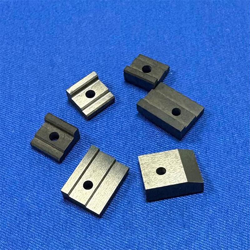
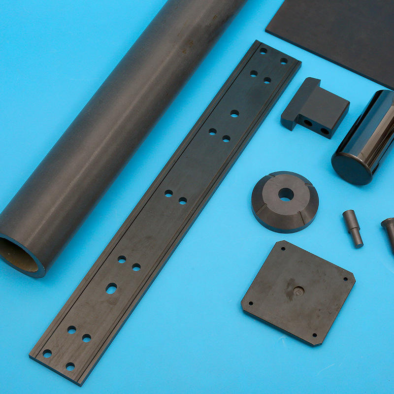
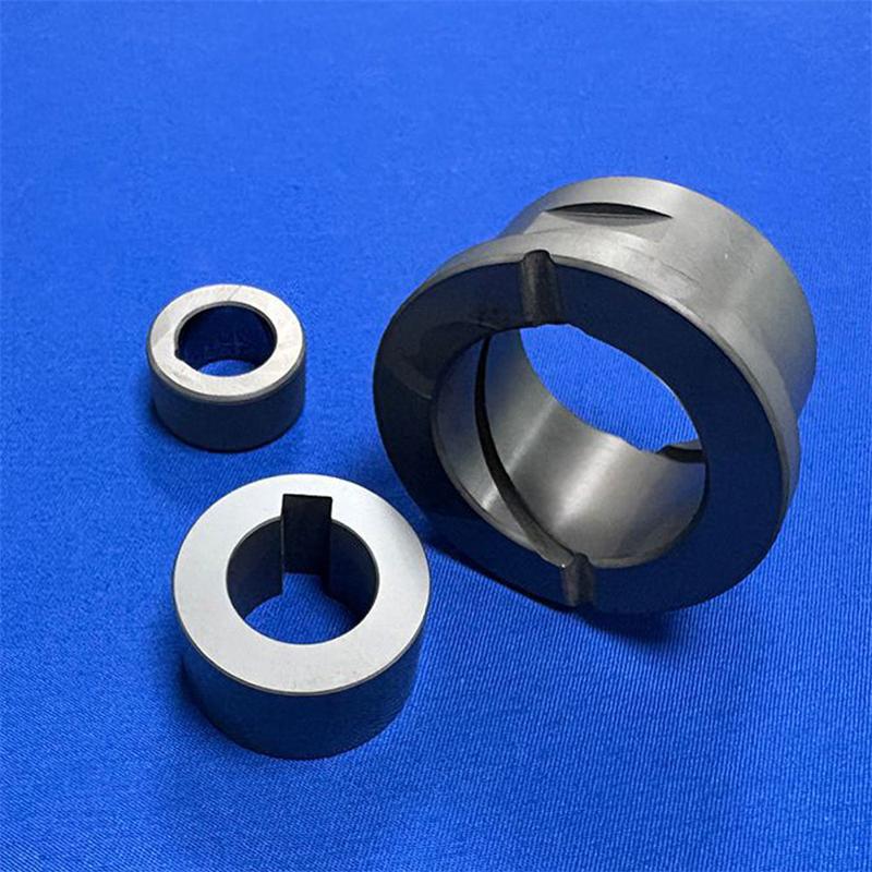
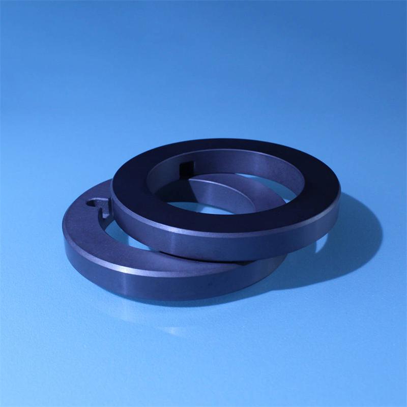
Brudeze Ceramics supplies and sells a wide range of high-quality quartz glass, including alumina ceramics, zirconia ceramics, silicon nitride ceramics, aluminum nitride ceramics, silicon carbide ceramics, boron carbide ceramics, bioceramics, machinable ceramics, etc. We can meet the customization requirements of various ceramic products.
Tags: boron carbide ceramics
PREVIOUS:Application of silicon nitride ceramics in the preparation of fine ceramics
NEXT:Application of silicon nitride ceramics in high-power optoelectronic field
CATEGORIES
LATEST NEWS
- Which is more wear-resistan...
- Are microcrystalline cerami...
- What is the difference betw...
- Compared to ordinary cerami...
- What are the main material ...
- Large sized microcrystallin...
- What is the maximum operati...
- Low dielectric constant mic...
- High hardness and wear-resi...
- Low expansion microcrystall...