
Photovoltaic ceramic perforated substrate is a core electronic packaging and heat dissipation carrier made of high-performance inorganic non-metallic materials such as high-purity alumina (Al ₂ O3), aluminum nitride (AlN), or silicon carbide (SiC) as carriers, and prepared through precision molding, high-temperature sintering, and micrometer level precision punching processes. As a key component in photovoltaic inverters, power modules, and battery etching equipment, it is perfectly adapted to high-frequency and high-power photovoltaic application scenarios with excellent insulation, high thermal conductivity, and extremely low thermal expansion coefficient. It is the “hidden cornerstone” that ensures the long-term stable operation of photovoltaic modules.
Requirements and Problem Solving
From the perspective of photovoltaic equipment manufacturers and component integrators, our photovoltaic ceramic perforated substrates mainly solve the following core problems for you:
Overcoming the bottleneck of heat dissipation and improving conversion efficiency: solving the problem of overheating of power devices caused by thermal conductivity differences in traditional FR4 or metal substrates, effectively reducing thermal resistance, significantly reducing the operating temperature of photovoltaic cells or IGBT modules, thereby improving energy conversion efficiency by 3% -5%.
Ensuring micrometer level accuracy and eliminating etching defects: To address the problem of uneven ion conduction in photovoltaic etching processes, we provide precision micropores with minimal aperture deviation and extremely high verticality, avoiding uneven etching and increased leakage rate of silicon wafers caused by hole displacement or blockage.
Enhancing extreme environmental reliability: Addressing the hidden dangers of substrate cracking and metal layer detachment in outdoor high-temperature, high humidity, and cold hot cycling environments for photovoltaic equipment, ensuring the mechanical stability and electrical insulation safety of components throughout their entire lifecycle.
Application and core advantages
Our photovoltaic ceramic perforated substrates are widely used in fields such as photovoltaic inverters, energy storage converters (PCS), photovoltaic cell etching machines, and automotive electronic IGBT module packaging. We have achieved a perfect combination of ceramics and metals through advanced DPC (direct copper plating), DBC, and AMB active metal brazing processes.
Advantages and Value:
Excellent thermal conductivity and insulation performance: Made of high-purity aluminum nitride or aluminum oxide substrate, the highest thermal conductivity can reach 170-260 W/(m · K), and the volume resistivity is ≥ 10 ¹⁶Ω· cm, ensuring high voltage insulation safety while efficiently dissipating heat.
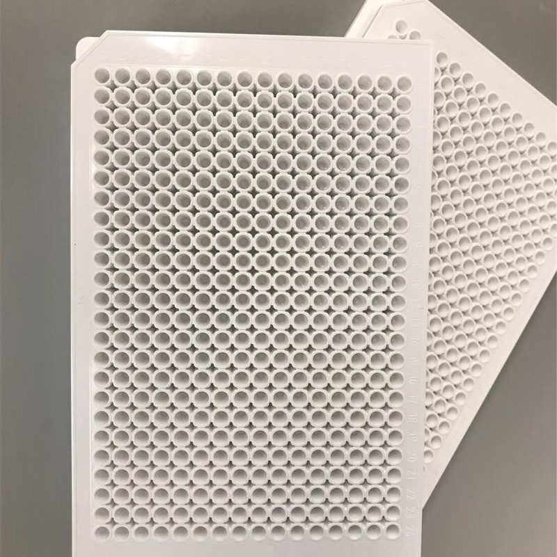
Micron level precision drilling process: By introducing ultrasonic assisted machining and high-precision laser drilling technology, micro hole machining with a minimum aperture of 20 μ m can be achieved. The hole spacing tolerance is controlled within ± 0.005mm, and the verticality error is less than 0.003mm, perfectly adapting to high-density integration requirements.
Excellent compatibility and weather resistance: The thermal expansion coefficient is highly matched with the silicon chip, greatly reducing the risk of solder joint fatigue caused by thermal stress; Simultaneously possessing strong resistance to chemical corrosion and acid and alkali.
Customization service for specifications and dimensions:
We are well aware of the differences in different photovoltaic application scenarios and provide comprehensive customized services:
Substrate selection: 96% alumina, high thermal conductivity aluminum nitride, or high-strength silicon nitride can be flexibly selected according to thermal conductivity and cost requirements.
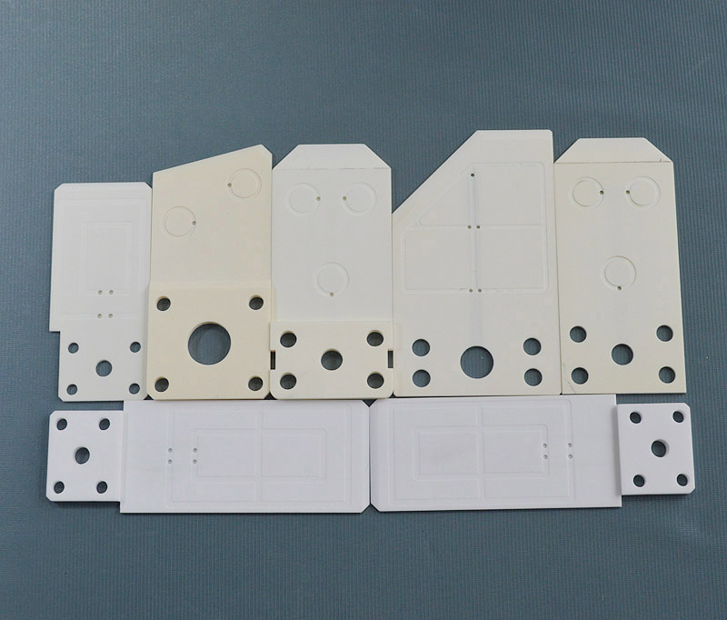
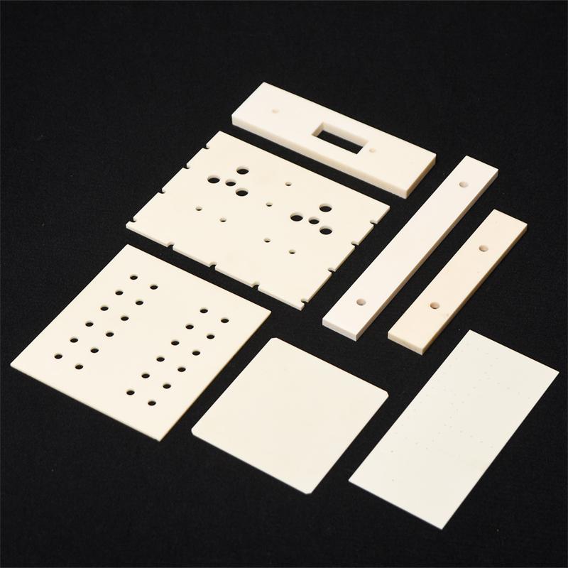
Size and thickness: Supports cutting of any size from microchip substrates to large power module substrates, with a thickness range covering 0.15mm to 5.0mm.
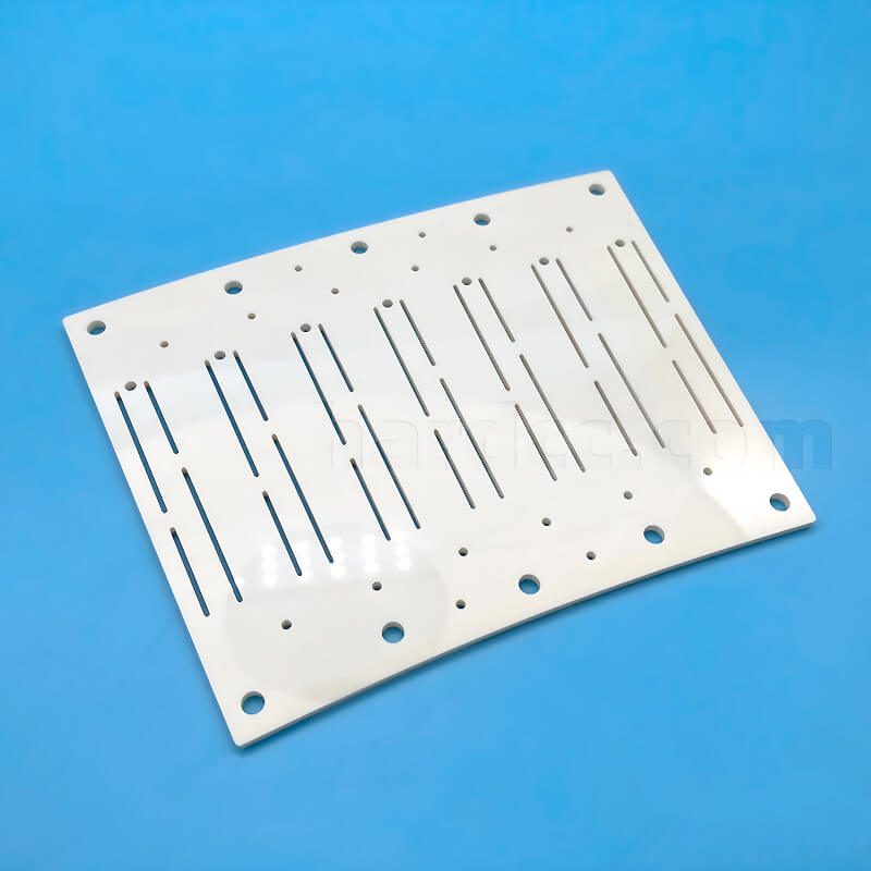
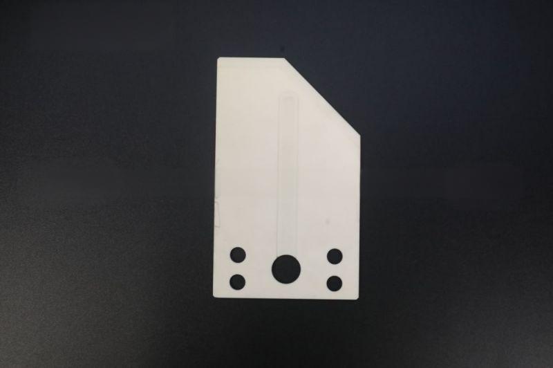
Customization of hole type: Supports processing of through holes, blind holes, buried holes, and irregular grooves, with a hole diameter range of 0.02mm-5.0mm for any customization.
Metalization process: Provides various surface treatments such as single-sided/double-sided copper plating, nickel gold plating, silver plating, etc. The copper thickness can be adjusted between 1oz and 20oz according to current carrying requirements.
Customer application case sharing (anonymous):
A certain photovoltaic equipment company encountered a serious yield crisis while producing TOPCon battery etching machines. The originally used silicon carbide ceramic base had excessive verticality of micropores and a deviation of 0.015mm in aperture due to traditional laser drilling, resulting in uneven ion distribution. This directly led to uneven etching of a batch of 100000 silicon wafers, resulting in a direct economic loss of over 4 million yuan and almost missing out on orders worth billions of yuan.
After introducing our customized photovoltaic ceramic punching substrate solution, the company adopted a precision punching process equipped with ultrasonic assisted machining technology. We carried out batch processing of 1200 φ 0.5mm micropores on a 500mm diameter silicon carbide substrate, successfully stabilizing the hole spacing tolerance within ± 0.003mm, controlling the verticality error below 0.002mm, and reducing the surface roughness to Ra0.1 μ m. In the end, the efficiency of the customer’s photovoltaic etching equipment significantly improved, and the substrate yield rate jumped from 85% to over 98%, completely solving the problem of etching uniformity. Not only did it recover huge losses, but it also enabled its product to occupy a technological high ground in the fierce market competition.
Choosing us means choosing lower electricity costs, higher photoelectric conversion efficiency, and more reliable equipment operation guarantee.
If you have customized needs for photovoltaic ceramic substrates, precision drilling, or heat dissipation packaging, please feel free to contact us at any time for exclusive technical solutions and sample testing!
Brudeze Ceramics supplies and sells a wide range of high-quality quartz glass, including alumina ceramics, zirconia ceramics, silicon nitride ceramics, aluminum nitride ceramics, silicon carbide ceramics, boron carbide ceramics, bioceramics, machinable ceramics, etc. We can meet the customization requirements of various ceramic products.
Tags: boron carbide ceramics
CATEGORIES
LATEST NEWS
- Can zirconia ceramic rods b...
- What Is the Minimum Toleran...
- Can Holes or Grooves Be Dri...
- How to Determine the Insula...
- What is the maximum operati...
- The antioxidant capacity of...
- What is the thermal shock r...
- What is the flexural streng...
- What are the advantages of ...
- What is the thermal conduct...