
Application of Zirconia Ceramics in Semiconductor Electronics
Zirconia (ZrO ₂) ceramics, especially yttrium stabilized zirconia (Y-TSZ), have become an indispensable key structural material in semiconductor manufacturing due to their excellent “ceramic steel” toughness, extremely low dielectric loss, excellent high temperature resistance, and zero metal ion precipitation characteristics. From wafer transfer arms to electrostatic suction cups (ESC), and then to plasma etching chamber components, high-purity zirconia ceramics effectively solve the problems of particle pollution, electrostatic damage, and strong corrosive gas erosion in ultra clean environments, and are the core guarantee for improving chip yield and equipment stability.
Frequently Asked Questions (FAQ)
Q1: Why is the semiconductor industry more inclined to use zirconia ceramics instead of alumina ceramics?
A: Although aluminum oxide (Al ₂ O3) has a lower cost, zirconium oxide (ZrO ₂) has higher fracture toughness (3-5 times that of aluminum oxide) and bending strength, and can withstand frequent mechanical and thermal shocks in semiconductor devices. In addition, zirconia has a higher dielectric constant, making it particularly suitable for scenarios such as electrostatic suction cups (ESCs) that require strong electrostatic clamping force. Its thermal expansion coefficient is closer to that of silicon wafers, which can reduce wafer warping caused by thermal stress.
Q2: Will zirconia ceramics be corroded in plasma etching environment?
A: Ordinary zirconia may undergo slight reactions in fluorine-containing plasma, but the semiconductor grade zirconia we provide has undergone special densification treatment and high-purity raw material screening (purity ≥ 99.9%), and can be optionally equipped with special surface coatings or modified formulas, significantly improving its resistance to corrosive gases such as CF ₄ and SF ₆, greatly extending component life and reducing downtime replacement frequency.
Q3: Can you provide customized sizes that meet SEMI standards?
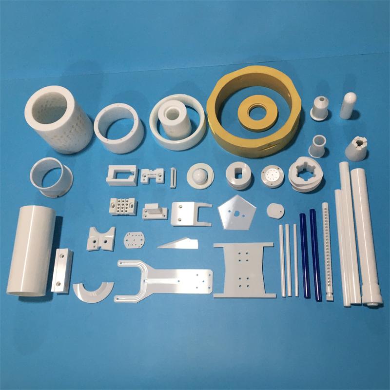
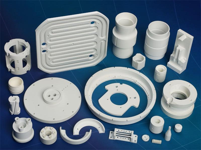
A: Yes, we strictly follow SEMI standards for production. In addition to standard specifications such as wafer grippers, nozzles, insulation rings, etc., we support comprehensive customization from micrometer level precision hole processing to large and complex structural components. We can provide drawing deepening, rapid prototyping, and bulk delivery services for special components on both 8-inch and 12 inch production lines.
Q4: How can zirconia ceramics help solve the problem of particle contamination on wafer surfaces?
A: Our zirconia ceramics are made using nanoscale powders and isostatic pressing technology. After sintering, the density is extremely high and the surface can be mirror polished (Ra ≤ 0.1 μ m). This ultra-low roughness surface not only makes it difficult to adsorb particles, but also generates very little debris during friction and has moderate hardness, which will not scratch expensive silicon wafers, ensuring the ultra cleanliness of the process.
User core needs and solutions
For semiconductor equipment manufacturers (OEMs) and wafer fabs (Fab), zirconia ceramic components are not only consumables, but also guardians of yield. It precisely solves your three most headache inducing core problems:
Zero tolerance for metal pollution: completely eliminate the precipitation of impurity ions such as iron and nickel from traditional metal components in high temperature or plasma environments, to avoid chip circuit short circuits or performance degradation.
Brittle fracture risk: By utilizing the high toughness of zirconia, the hidden danger of ceramic components being prone to breakage and slag falling during automated high-speed transmission, cleaning, and maintenance can be solved, ensuring the continuous operation of the production line.
Static control challenge: By precisely regulating the resistivity of materials, providing multiple options from insulation to dissipation, perfectly balancing the clamping force of electrostatic suction cups with the safety of wafer removal, and preventing damage to microcircuits caused by electrostatic discharge (ESD).

The core value of zirconia in the semiconductor field
Ultimate breakthrough in material performance
The yttrium stabilized tetragonal zirconia polycrystal (Y-TSZ) we selected represents the highest level of structural ceramics currently available
Ultra high toughness: fracture toughness K {IC} geq 8.0, text {MPa}cdottext {m}^{1/2}, Bending strength geq 900, text {MPa}, capable of withstanding harsh mechanical loads.
Excellent electrical properties: high volume resistivity (>10 ^ {14} at room temperature, Omegacdottext {cm}), high dielectric strength, making it an ideal insulation and electrostatic control material.
Low thermal conductivity and thermal shock resistance: As a thermal barrier material, it can effectively isolate high-temperature areas, protect external precision mechanisms, and resist thermal shock caused by rapid temperature rise and fall.
Non magnetic characteristics: completely non-magnetic, suitable for special process environments such as electron beam lithography that are sensitive to magnetic fields.
Key application scenarios and value
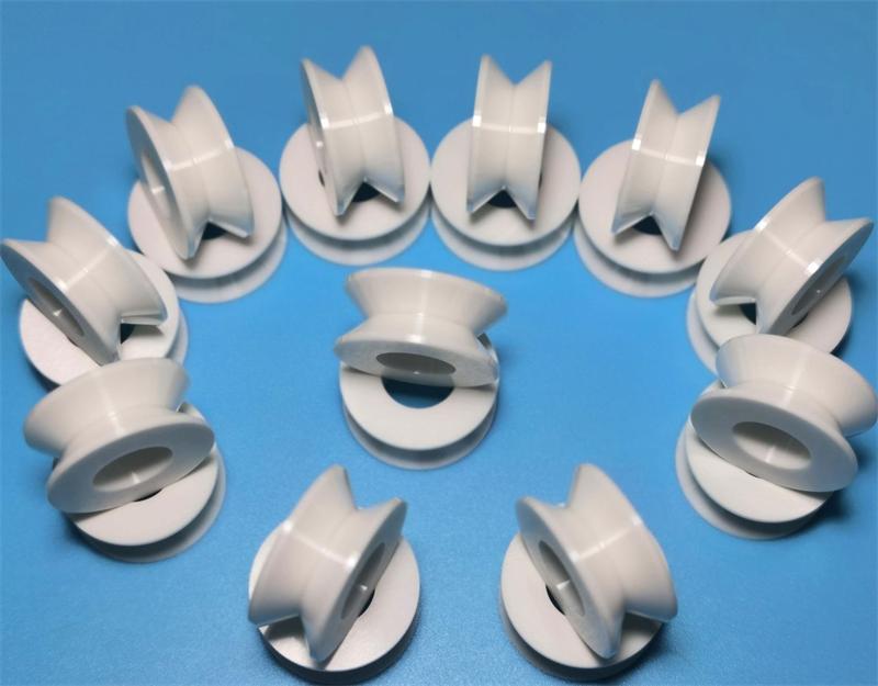
End effectors/Robot Arms:
Value: Lightweight design reduces robot load, improves acceleration and rhythm; High rigidity ensures transmission accuracy; Smooth surface to prevent wafer from slipping or scratching.
Electrostatic Chuck (ESC):
Value: Utilizing the high dielectric constant of zirconia to achieve stronger electrostatic forces, ensuring the flatness of wafers during etching/deposition processes; Uniform resistivity distribution ensures consistency in wafer temperature control.
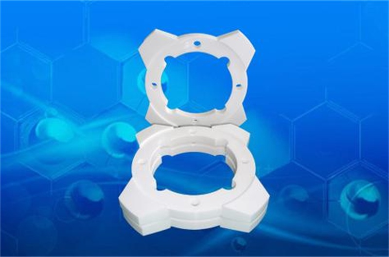
Plasma chamber components (Focus Rings, Showerheads):
Value: Resistant to plasma erosion, reduces particle generation, extends cleaning cycle, and directly improves equipment utilization (Uptime).
Precision insulation and positioning components:
Value: Provides stable electrical insulation and mechanical support in high-temperature diffusion furnaces or ion implantation machines, with excellent dimensional stability.
Customer application case sharing
Case 1: A leading 12 inch wafer foundry in China (anonymous)
Background challenge: In the dry etching process of advanced logic chips, the imported alumina focus ring used by the factory experiences severe edge peeling every 150 hours of operation in a high-density plasma environment, producing a large number of micrometer sized particles, resulting in a skyrocketing defect density on the wafer surface, and frequent shutdowns for replacement, seriously affecting production capacity.
Solution: We have developed a specially designed high-density zirconia composite focusing ring for it. By adjusting the grain size distribution and adding trace rare earth additives, the anti sputtering ability of the material in fluorine based plasma has been significantly improved. At the same time, the surface was polished at the nanoscale.
Implementation effect: After the new component was launched, its service life was extended to over 600 hours (increased by 4 times), and the particle generation rate was reduced by 90%. According to customer statistics, this improvement alone saves approximately 1.2 million yuan in spare parts costs for the production line annually, and indirectly increases output value by tens of millions of yuan by reducing unplanned downtime.
Case 2: An internationally renowned semiconductor equipment manufacturer (anonymous)
Background challenge: In its latest developed wafer transfer robot, a lightweight and highly resilient end effector is needed to adapt to high-speed transfer of ultra-thin wafers (thickness<100 μ m). The original quartz material is fragile, while silicon carbide has a high cost and long processing cycle.
Solution: We provide customized thin-walled zirconia ceramic arms. By utilizing the high fracture toughness of zirconia, the wall thickness is reduced to 3mm without sacrificing strength, and the weight is 15% lighter than alumina. A special vacuum adsorption microporous array is also designed.
Implementation effect: The component successfully passed the customer’s rigorous fatigue test of millions of times without any cracks. Its excellent dynamic performance has increased the robot’s transmission speed by 20%, and there has been no wafer breakage accident caused by arm breakage throughout the year, making it a standard configuration for this equipment model.
Are you looking for a high-performance zirconia ceramic solution that can improve chip yield and extend equipment lifespan?
Contact our technical expert team immediately for sample testing and customized engineering evaluation. Let us use the ultimate ceramic craftsmanship to help you lead the precision race in semiconductor manufacturing!
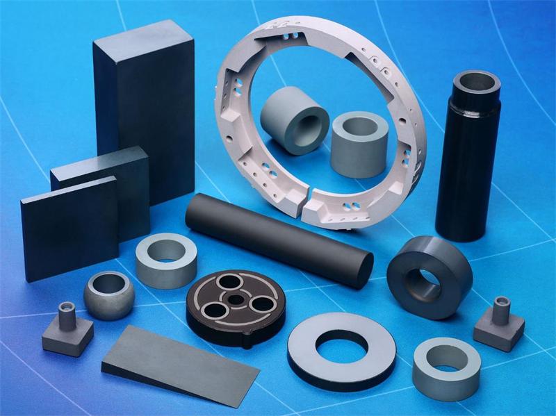
Brudeze Ceramics supplies and sells a wide range of high-quality quartz glass, including alumina ceramics, zirconia ceramics, silicon nitride ceramics, aluminum nitride ceramics, silicon carbide ceramics, boron carbide ceramics, bioceramics, machinable ceramics, etc. We can meet the customization requirements of various ceramic products.
Tags: boron carbide ceramics
PREVIOUS:Application of Zirconia Ceramics in Petrochemical Industry
NEXT:Application of Zirconia Ceramics in Mechanical and Industrial Manufacturing
CATEGORIES
LATEST NEWS
- High temperature resistant ...
- High grinding zirconia cera...
- Pollution free zirconia cer...
- High purity zirconia cerami...
- Low wear zirconia ceramic b...
- High hardness zirconia cera...
- High density zirconia ceram...
- Electric field sintering zi...
- Magnetic field sintering zi...
- Activated sintered zirconia...