
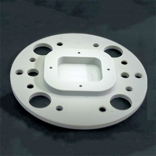
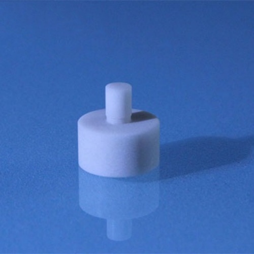
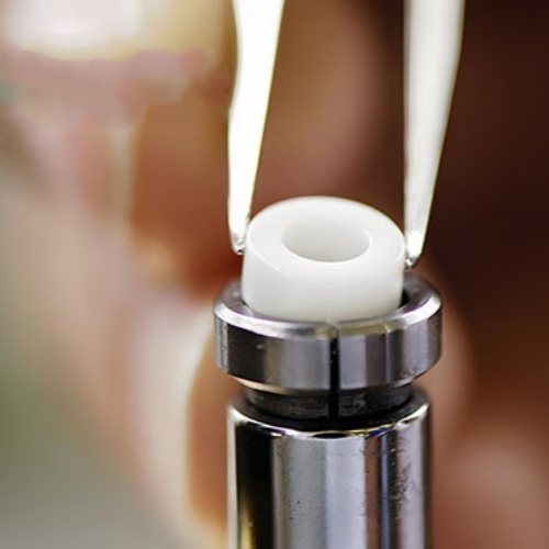
Customized ceramic packaging testing probe station is a high-precision equipment designed specifically for the semiconductor packaging testing field, mainly used for electrical performance testing, aging testing, burning and other operations on chips. Its core components are made of high-performance ceramic materials, which have excellent insulation, thermal stability, and mechanical strength.
The material of this probe station is machinable ceramic MACOR, which not only has the characteristics of ceramics, but also can be cut to meet the requirements of complex structures and high precision. The processing flow includes multiple stages such as powder, granulation, molding, sintering, precision machining, testing, and cleaning to ensure the high quality and performance of the product.
Application area
Customized ceramic sealing probe stations are widely used in the following fields:
- Semiconductor industry: Used for chip packaging testing equipment, capable of meeting the testing needs of different packaging forms (such as QFN, DFN, BGA, etc.).
- Integrated circuit manufacturing: Suitable for testing, burning, aging, and other processes of integrated circuits to ensure performance verification of chips at different stages of the manufacturing process.
- Optoelectronics field: It can be used for testing optoelectronic devices such as LED, LCD, solar cells, etc., to meet their special electrical and optical testing requirements.
- Scientific research: Used in laboratories of universities and research institutions for material property research, device performance testing, etc.
Customized service
Customized ceramic sealing probe station provides comprehensive customization services to meet customers’ personalized needs:
- Structural customization:
-Size and shape: Customize the size and shape of the probe station based on the chip packaging size and testing requirements provided by the customer.
-Probe layout: Based on the pin layout of the chip, design a reasonable arrangement of probes to ensure the accuracy and reliability of testing.
-Special structure: such as flip top structure, Open top structure, etc., which facilitates the loading, unloading, and testing operations of chips. - Performance customization:
-Temperature range: The conventional temperature range is -55 ° C~+180 ° C, and higher or lower temperature probe stations can be customized according to customer needs.
-Frequency range: The conventional frequency range is 1GHz~5GHz, and higher frequency probe stations can be customized to meet high-frequency testing requirements.
-Probe materials: Multiple probe material options are available, such as tungsten, beryllium copper, etc., to meet different testing requirements.
-Probe specifications: There are multiple specifications available for needle tip diameter, such as 5um, 10um, 25um, etc. - Function customization:
-Testing function: Customize corresponding testing function modules based on customer testing projects, such as I-V testing, C-V testing, RF testing, etc.
-Automation function: It can be equipped with an automated testing system to achieve automatic loading and unloading, testing, and data collection of chips.
-Additional functions: such as needle cleaning, grinding, and blowing functions to improve testing efficiency and probe lifespan.
The customized ceramic packaging and testing probe station, with its high performance, high precision, and flexible customization services, has become an indispensable equipment in the field of semiconductor packaging and testing. It can meet the diverse needs of different customers in different application scenarios, providing reliable solutions for chip manufacturing and testing.
Brudeze Ceramics supplies and sells a wide range of high-quality quartz glass, including alumina ceramics, zirconia ceramics, silicon nitride ceramics, aluminum nitride ceramics, silicon carbide ceramics, boron carbide ceramics, bioceramics, machinable ceramics, etc. We can meet the customization requirements of various ceramic products.
Tags: boron carbide ceramics
CATEGORIES
LATEST NEWS
- What are the applications o...
- Where is the wide applicati...
- What are the properties of ...
- What are the main aspects o...
- What are the main aspects o...
- What is zirconia ceramic fi...
- What are the methods for pr...
- What are the difficulties i...
- What are the advantages of ...
- What are the applications o...